If you’ve ever worked in semiconductor manufacturing, you know that even the tiniest defect in a wafer graphite carrier can derail an entire production run—leading to scrap wafers, wasted energy, and missed delivery deadlines. As a third-generation supplier specializing in custom and standard wafer graphite carriers, I’ve spent the last 18 years standing alongside our clients in fabs and R&D labs, walking through every single carrier before it ships out. Most of the questions I get on the floor aren’t about how to make a carrier—they’re about how to check one once it’s in use, or how to spot a defect before it becomes a crisis. Today, I want to pull back the curtain on the detection processes we’ve refined over decades, the common defects we see every day, and how you can catch issues early to keep your line running smooth. Wafer Graphite Carrier
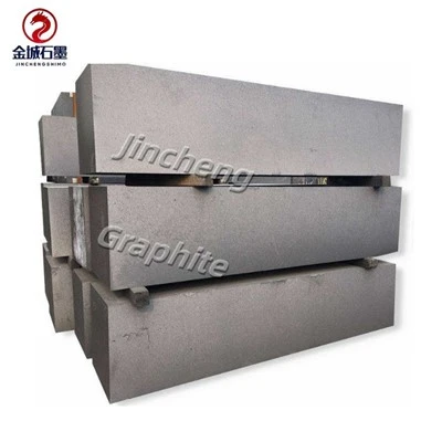
Let’s start with a quick reality check: wafer graphite carriers aren’t just blocks of graphite. They’re precision tools that hold 25, 50, even 100 wafers at a time through high-temperature processes like diffusion, etching, and chemical vapor deposition (CVD). A single defect—even a micro-crack, a tiny surface bump, or an out-of-spec pocket—can throw an entire batch of wafers off, costing clients tens of thousands of dollars in materials and downtime. Early in my career, I made a mistake: we shipped a carrier with a barely noticeable surface pit, and it snagged a 300mm wafer mid-process, shattering it and shutting down a 150-line fab for 12 hours. That day taught me that detection isn’t a one-and-done step—it’s a continuous, layered process that starts before the carrier even leaves our facility and continues through its entire lifecycle in your fab.
First, let’s break down the two core categories of defects we deal with: manufacturing defects (the ones that happen when we make the carrier) and in-service defects (the ones that show up from wear and tear over time). Both need different detection approaches, and both are critical to address.
Manufacturing defects are the ones we catch before a carrier ever hits your shipping pallet. The first line of defense is visual inspection, but not the quick, once-over visual you might do with a paper clip. We use high-resolution digital microscopes calibrated to 10-micron resolution—enough to see a grain of sand in a pocket, or a micro-crack that’s 1/100 the width of a human hair. Last month, we ran a batch of 200mm carriers for a client in Austin, and during this step, we found four carriers with tiny surface voids in the pocket edges. Those voids wouldn’t have caused a problem at room temperature, but at 1,000°C, the graphite would expand, and the void would turn into a crack that would scratch a wafer. We pulled those carriers, re-machined the edges, and sent them back for a second inspection before they left. It’s tedious, but it’s non-negotiable.
But visual inspection only catches surface defects. What about internal issues? That’s where non-destructive testing (NDT) comes in. For carriers over 300mm, we use ultrasonic testing to scan through the entire graphite block, looking for internal delaminations or voids that aren’t visible from the outside. A few years ago, we had a new graphite supplier send us a batch of raw blocks with hidden internal voids—voids that were too small to see when we machined them, but would have caused the carrier to warp at high temperatures when we ran a 50-waver batch. Ultrasonic testing caught all of them, and we switched to a new supplier that same week. We also use thermal imaging for custom carriers with complex geometries—we heat the carrier to a process temperature and scan for hot spots, which indicate gaps or defects in the graphite matrix that would affect uniform heating across the wafers.
Now, moving to in-service defects—this is the stuff our clients come to us with most often, because it’s the defects that show up while the carrier is working for them. The most common in-service defect is surface contamination, and it’s almost always caused by tiny particles flaking off the carrier’s surface. Graphite is porous by nature, and even after we coat carriers with silicon carbide (SiC) or pyrolytic carbon (PyC) for durability, repeated thermal cycling causes the coating to wear thin, leaving graphite exposed. Those tiny graphite particles stick to wafer surfaces, causing electrical shorts or scratches. We tell every client to do a weekly surface check on their carriers using a particle counter—even a particle as small as 1 micron can ruin a 200mm microchip. If the particle count on a carrier goes above 100 particles per square centimeter, it’s time to re-coat or replace the carrier.
Another super common in-service defect is pocket wear. Each time a carrier is loaded and unloaded, the pockets that hold the wafers rub against the wafer edges. Over 500-1,000 process cycles, those pockets can wear out of spec—meaning the pocket is too deep, too shallow, or tilted. If a pocket is too shallow, the wafer can slip out during high-speed transport; if it’s tilted, the wafer will be uneven, leading to non-uniform etching or deposition. We recommend using a coordinate measuring machine (CMM) to check pocket dimensions every 100 cycles. CMM is a precision tool that measures every pocket’s depth, width, and angle down to 1 micron, so you can spot wear before it becomes a problem. Last quarter, a client in Taiwan noticed their 300mm carriers had started having wafer misalignment issues—their CMM check showed pockets had worn 15 microns out of spec in just 800 cycles, which is almost double the acceptable limit. We re-machined and re-coated the entire set, and their misalignment issues went away immediately.
Cracks are the most dangerous in-service defects. Micro-cracks can start at the pocket edges or at the carrier’s mounting points, and they can spread quickly during thermal cycling. The problem is, micro-cracks are often invisible to the naked eye until they’re large enough to cause a failure. We recommend using dye penetrant testing for this—this is a simple, low-cost method where you spray a red or blue dye on the carrier, wipe it off, and then apply a developer. The dye seeps into any cracks, and the developer makes them visible under UV light. We teach all our clients how to do this in their own fab, because it’s fast and can catch cracks before they break a wafer. A client in South Korea used this method last year and caught a crack in a carrier that had only run 600 cycles—they were able to replace it before it caused $100k worth of wafer scrap.
Now, let’s talk about a mistake we see clients making all the time: not calibrating their detection tools. If your CMM isn’t calibrated every three months, its measurements are off, and you’ll miss pocket wear. If your particle counter hasn’t been serviced, it’ll undercount particles, and you’ll think your carriers are clean when they’re not. We offer free calibration checks for all the tools our clients use for carrier inspection—we send our technician out once a year to calibrate CMMs, particle counters, and microscopes, because we want our clients to succeed as much as they want to succeed themselves.
One thing I always emphasize is that every fab’s carrier needs are different. A 200mm fab running low-temperature processes won’t need the same inspection as a 300mm fab running 1,200°C CVD processes. That’s why we work with each client to build a custom inspection plan tailored to their specific processes, equipment, and quality standards. For example, a research lab running small-batch semiconductor experiments might only need visual inspection and dye penetrant testing, while a high-volume production fab with 100+ carriers running 24/7 needs ultrasonic testing, CMM checks, and thermal imaging on a regular schedule.
I also want to share some common pitfalls we’ve learned to avoid over the years. First, don’t wait for a failure to inspect your carriers. We’ve seen clients wait until a wafer is scratched before checking their carriers, and by that point, they’ve already lost thousands of dollars. Second, don’t skimp on carrier maintenance. Re-coating a carrier every 1,000 cycles costs a fraction of the cost of replacing a batch of wafers. Third, don’t use a one-size-fits-all inspection plan. A carrier for MEMS wafers has different requirements than a carrier for power semiconductors, so your inspection needs should match that.

At the end of the day, wafer graphite carriers are the unsung heroes of semiconductor manufacturing. They don’t get the same press as advanced lithography machines or etching tools, but without them, none of those processes work. As a supplier, our job isn’t just to make carriers—it’s to help our clients detect defects early, reduce downtime, and keep their production lines running. If you’re dealing with carrier-related issues, or if you need help building an inspection plan that works for your fab, I’d love to talk. We don’t just sell carriers—we partner with our clients to solve problems, and that starts with being transparent about what to look for, and how to catch it before it costs you.
Graphite Ring References:
- Semiconductor Manufacturing International Corporation. Wafer Handling Equipment Specification and Inspection Standards. 2021.
- ASM International. Non-Destructive Testing of Carbon and Graphite Materials for High-Temperature Applications. 2019.
- IEEE Transactions on Semiconductor Manufacturing. Quality Control for Wafer Carriers in 300mm Fabs. Vol. 32, No. 2, 2019.
- Chemical Vapor Depulsion Society. Coating Performance of Graphite Carriers for Semiconductor Processing. 2020.
- International Technology Roadmap for Semiconductors. Advanced Packaging and Manufacturing Equipment, 2022 Edition.
Huixian Jincheng Abrasive Mold Factory
As one of the most professional wafer graphite carrier manufacturers and suppliers in China, we have world-leading production equipment and strong manufacturing capabilities. Please rest assured to buy durable wafer graphite carrier for sale here from our factory. Quality products and reasonable price are available.
Address: Mengzhuang Town, Huixian City, Henan Province
E-mail: graphite.jc@gmail.com
WebSite: https://www.graphite-jc.com/
